We would like to keep you up to date with the latest information on SSI International 2023 by sending you push notifications.

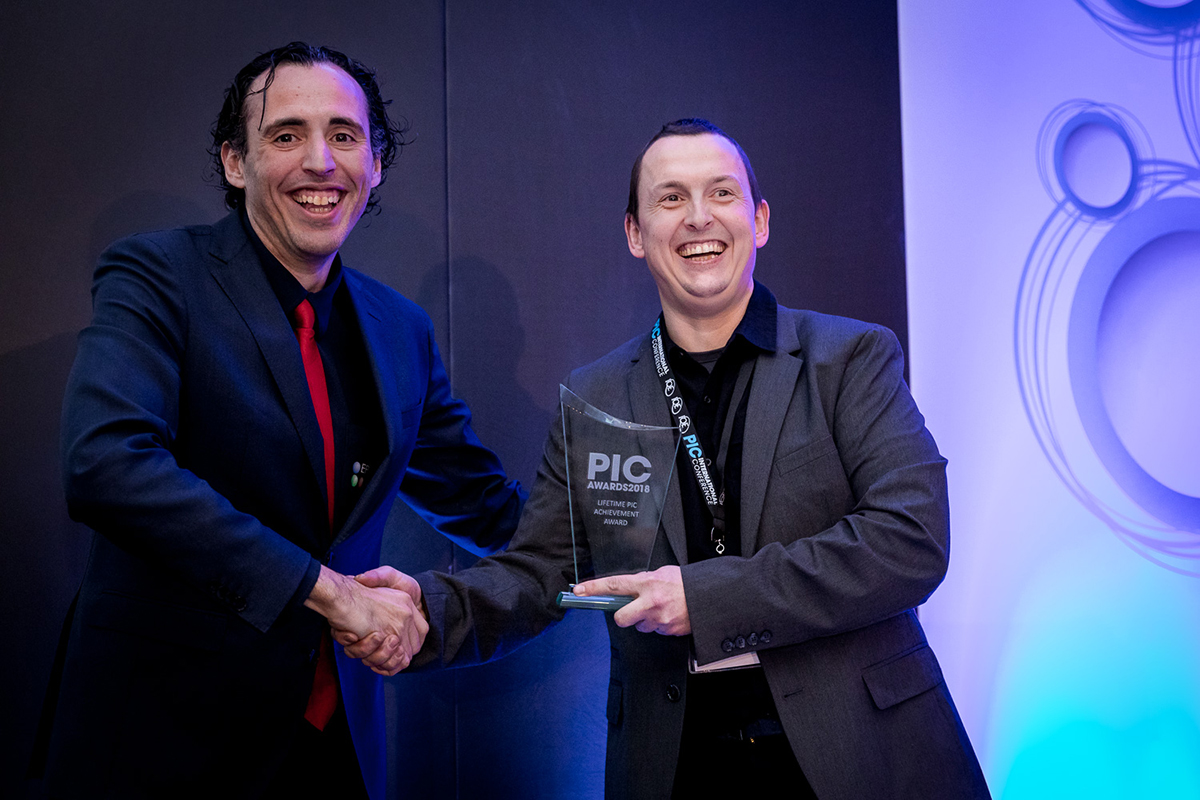
Attendees Applaud New HES International Conference
Advanced sensor technologies took center stage at HES International in Brussels, pointing towards a future of integrated opto and electro technologies in IoT, autonomous transport and wide-ranging cyber physical systems.
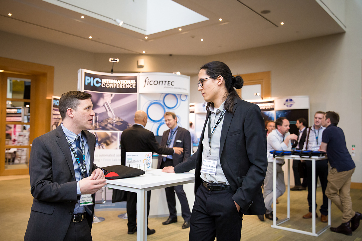
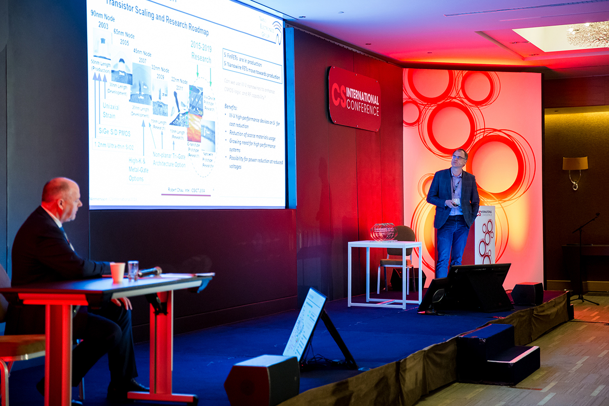
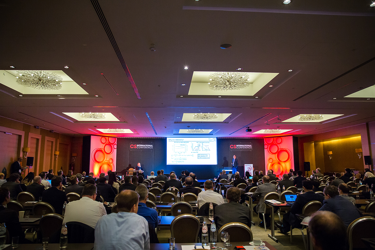
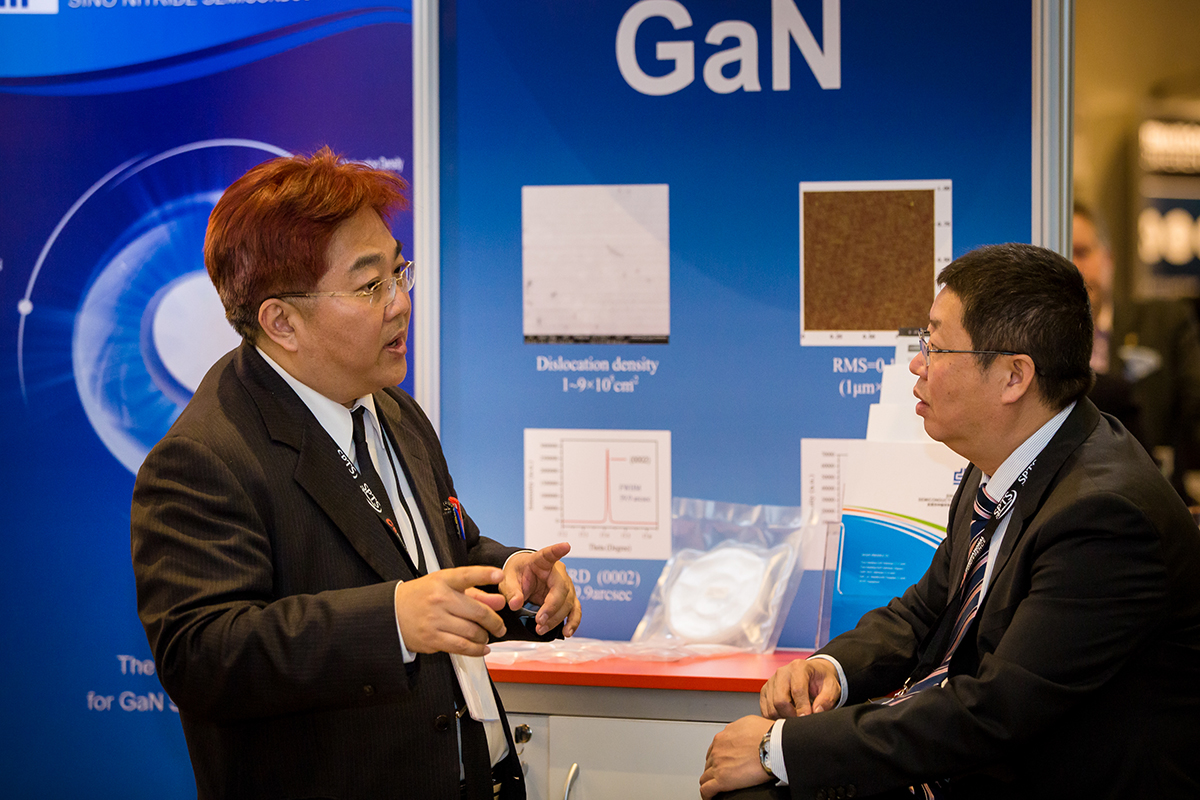
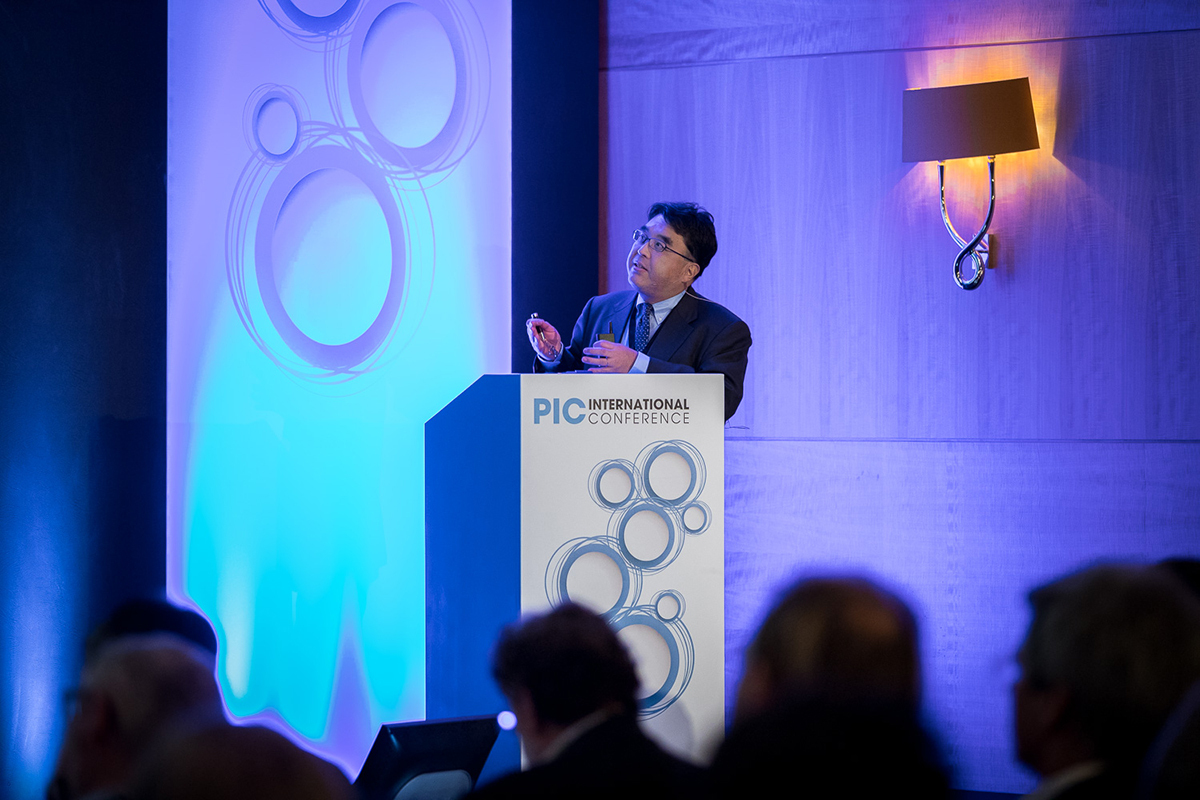
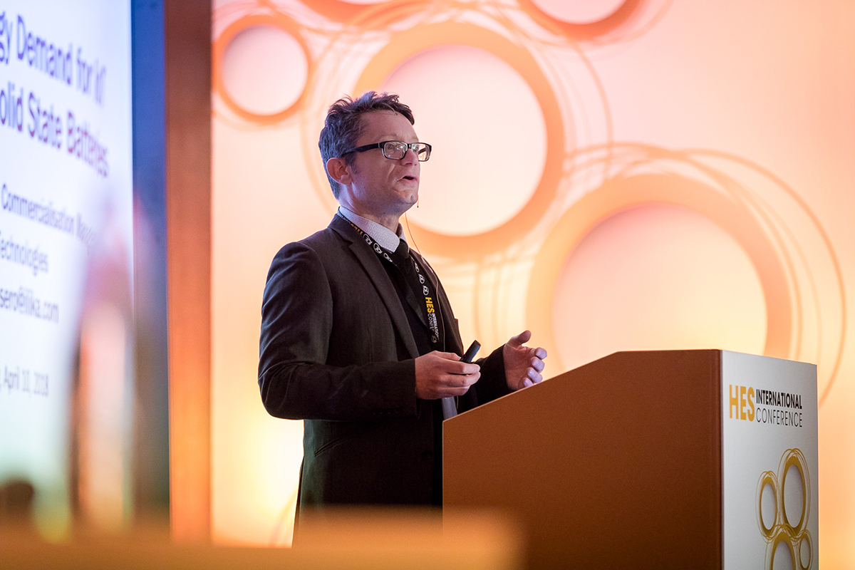
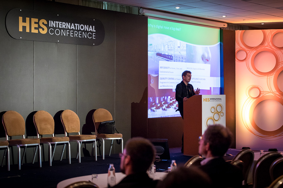
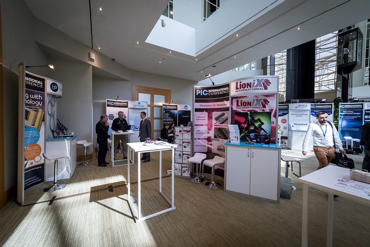
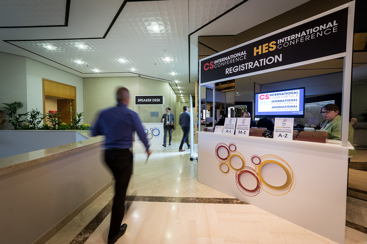
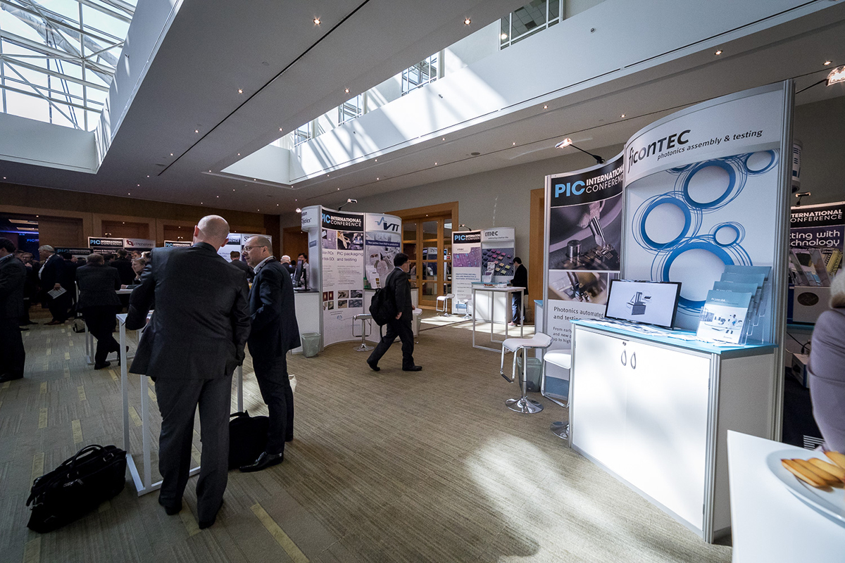
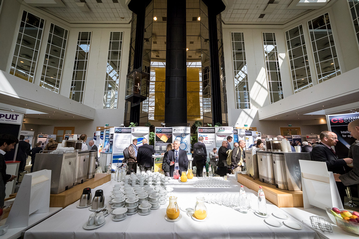
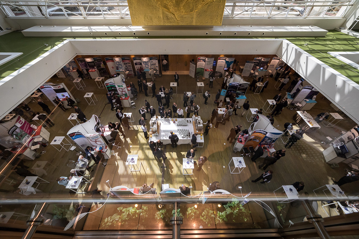
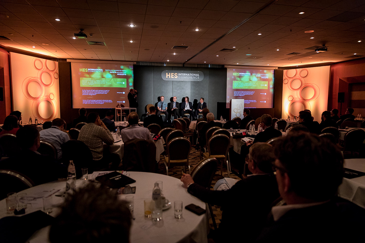
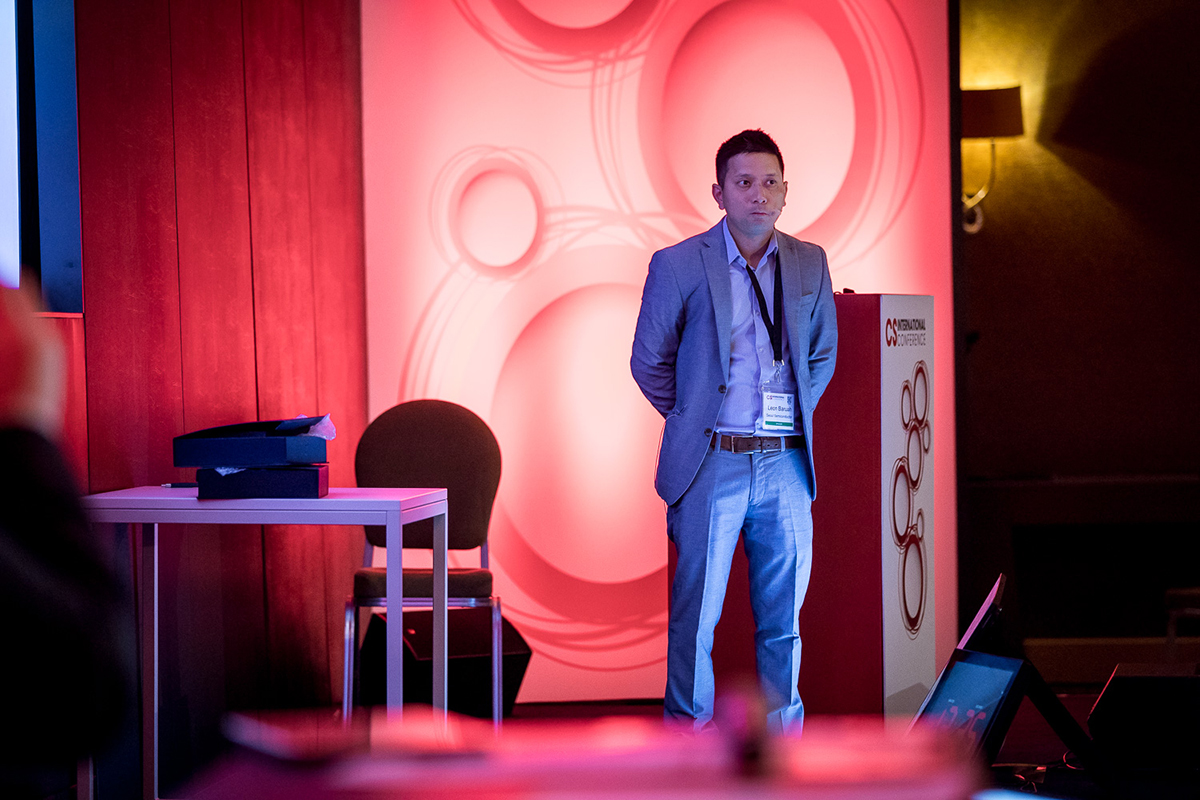
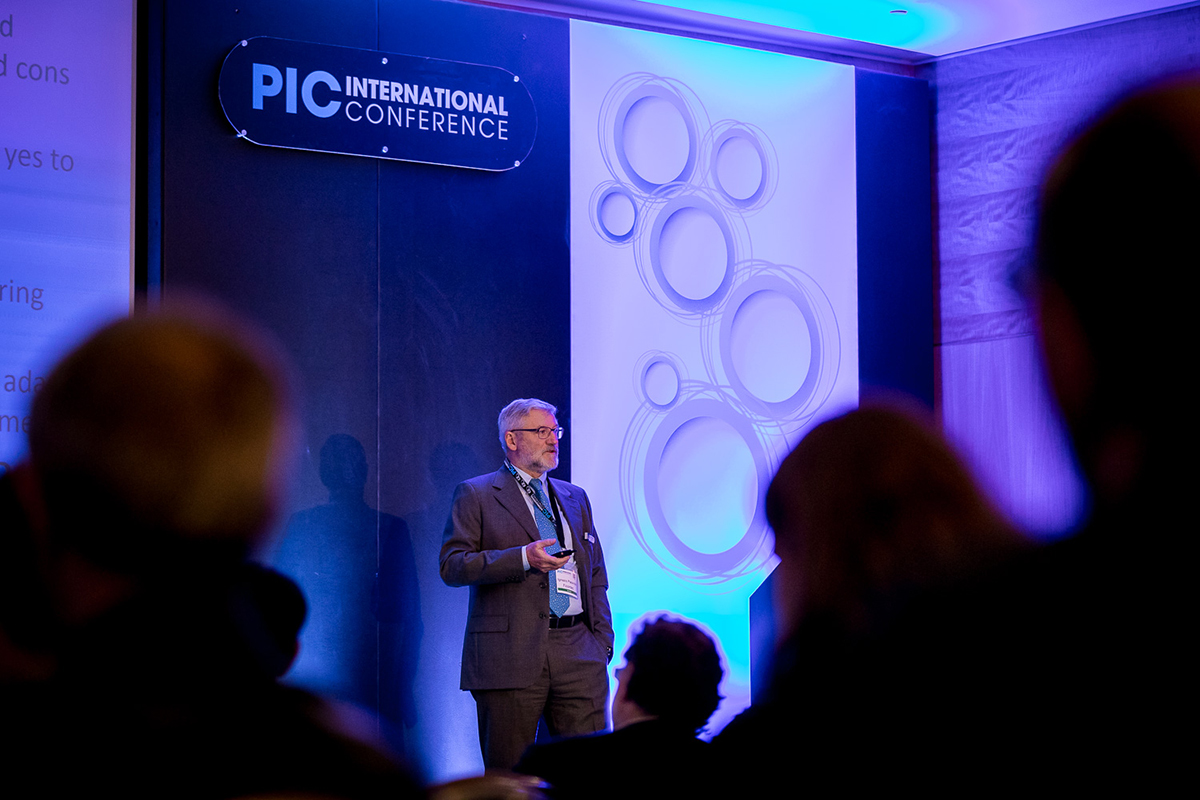
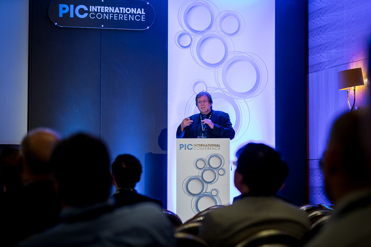
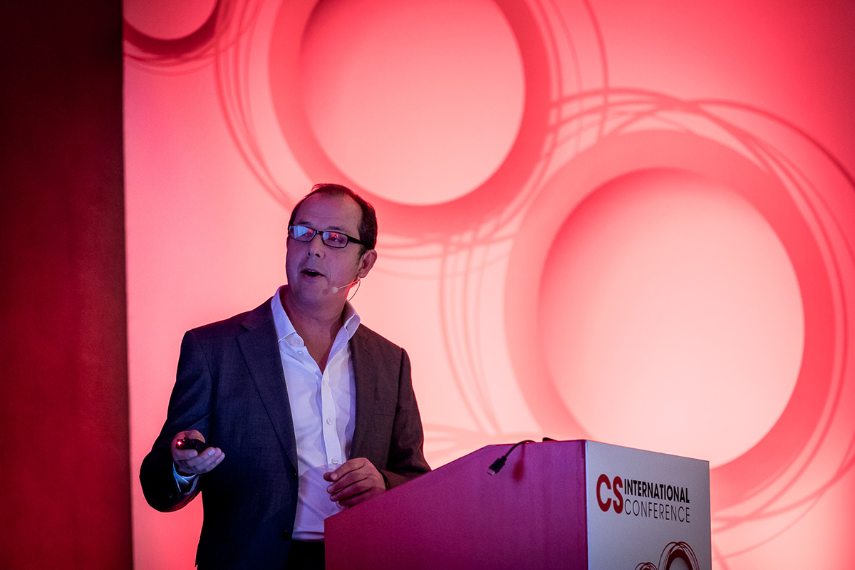
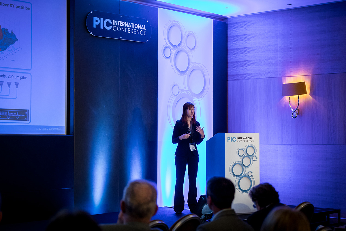
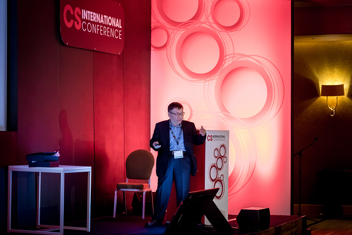
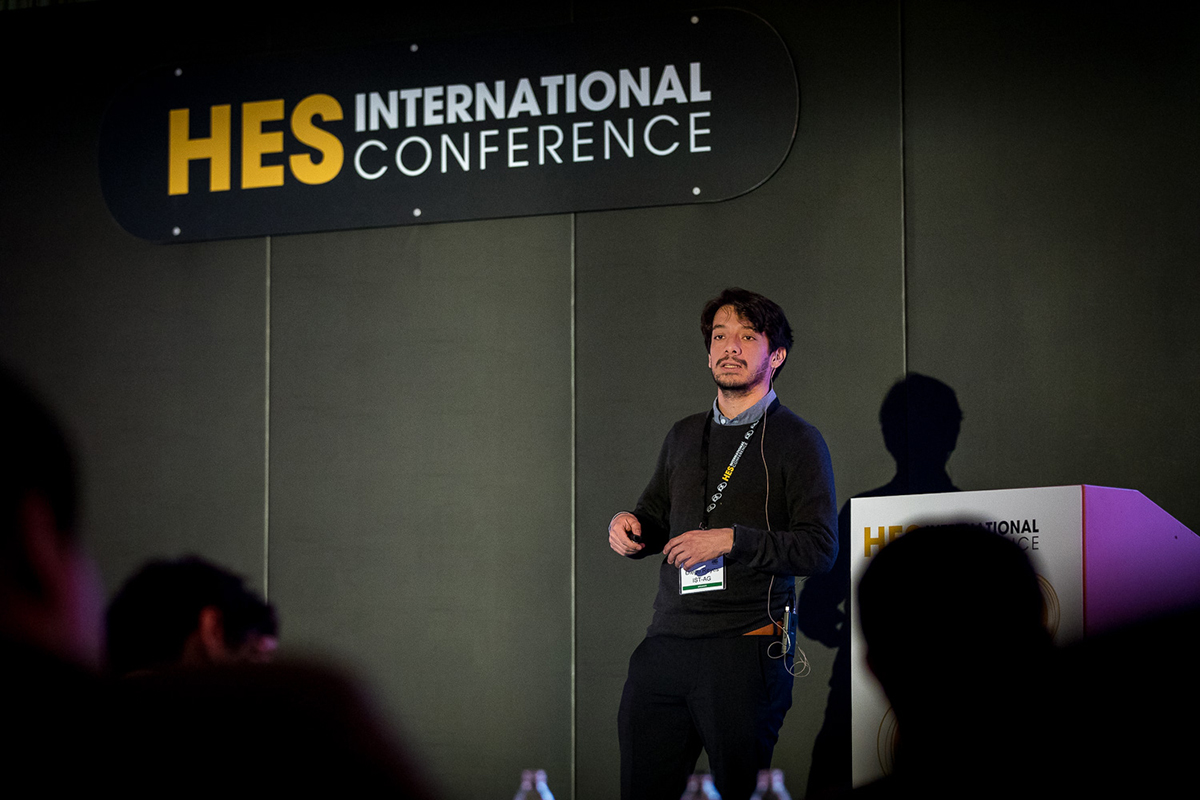
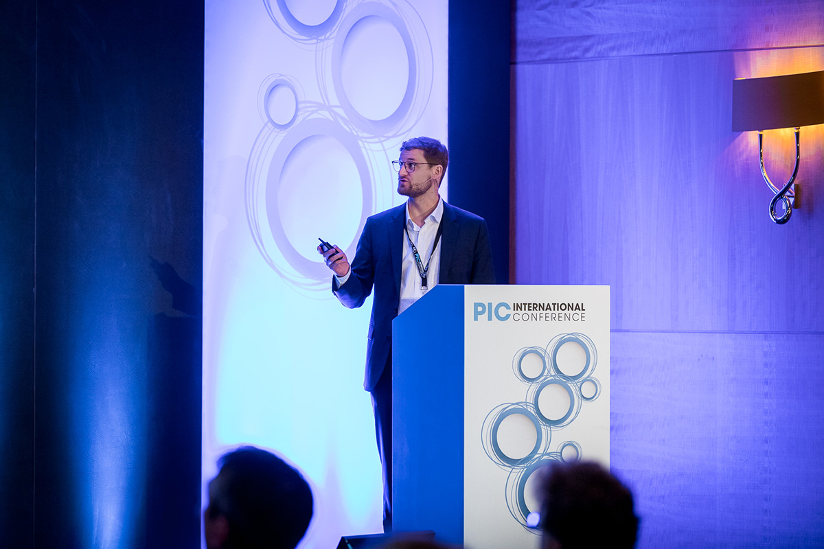
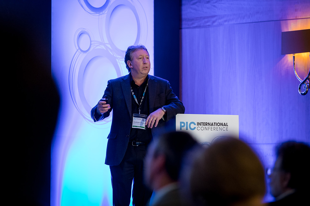
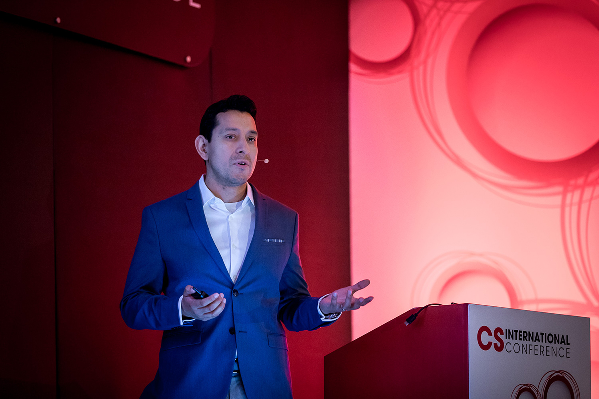
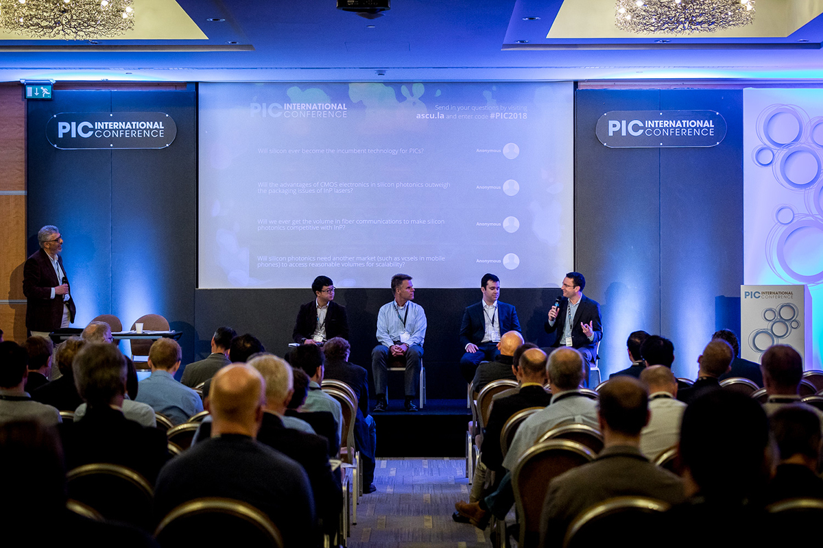
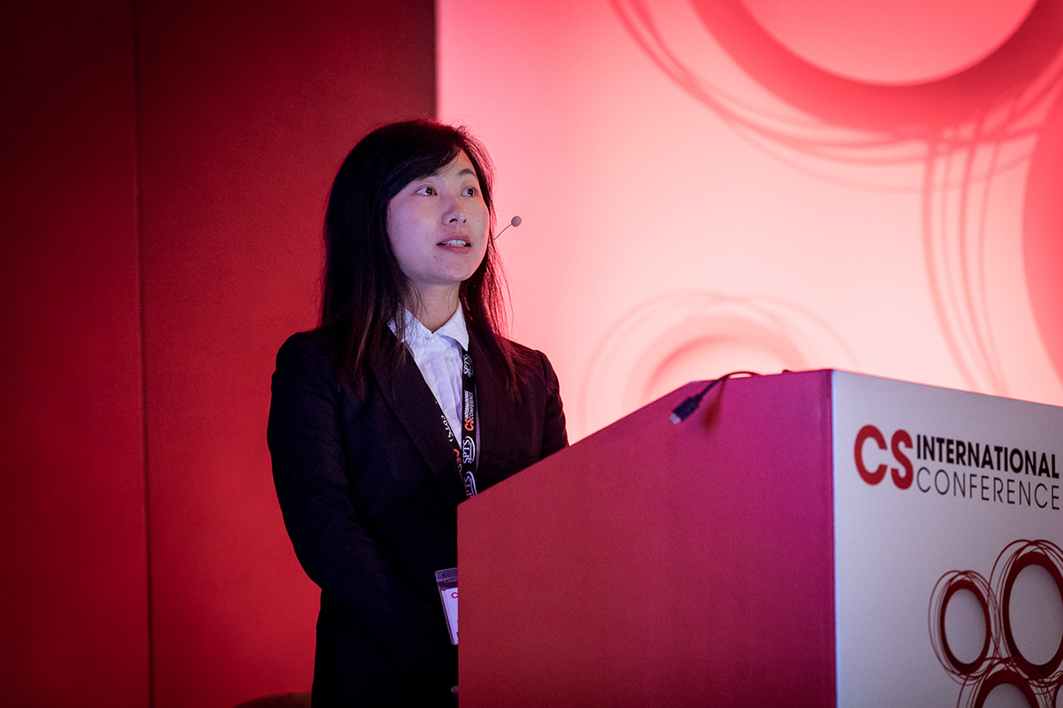
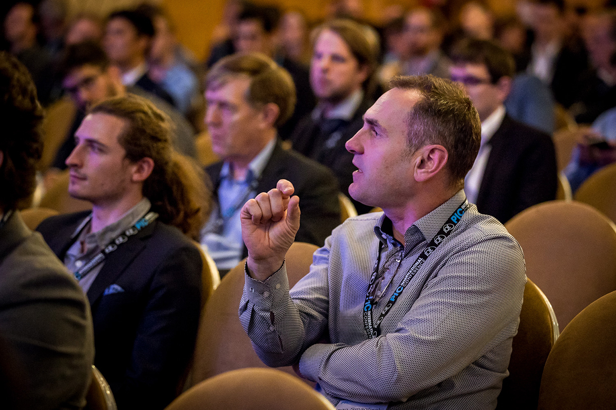
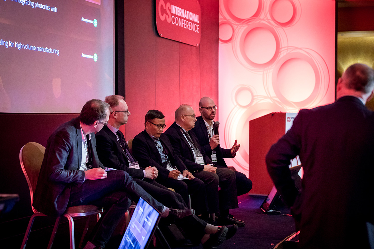
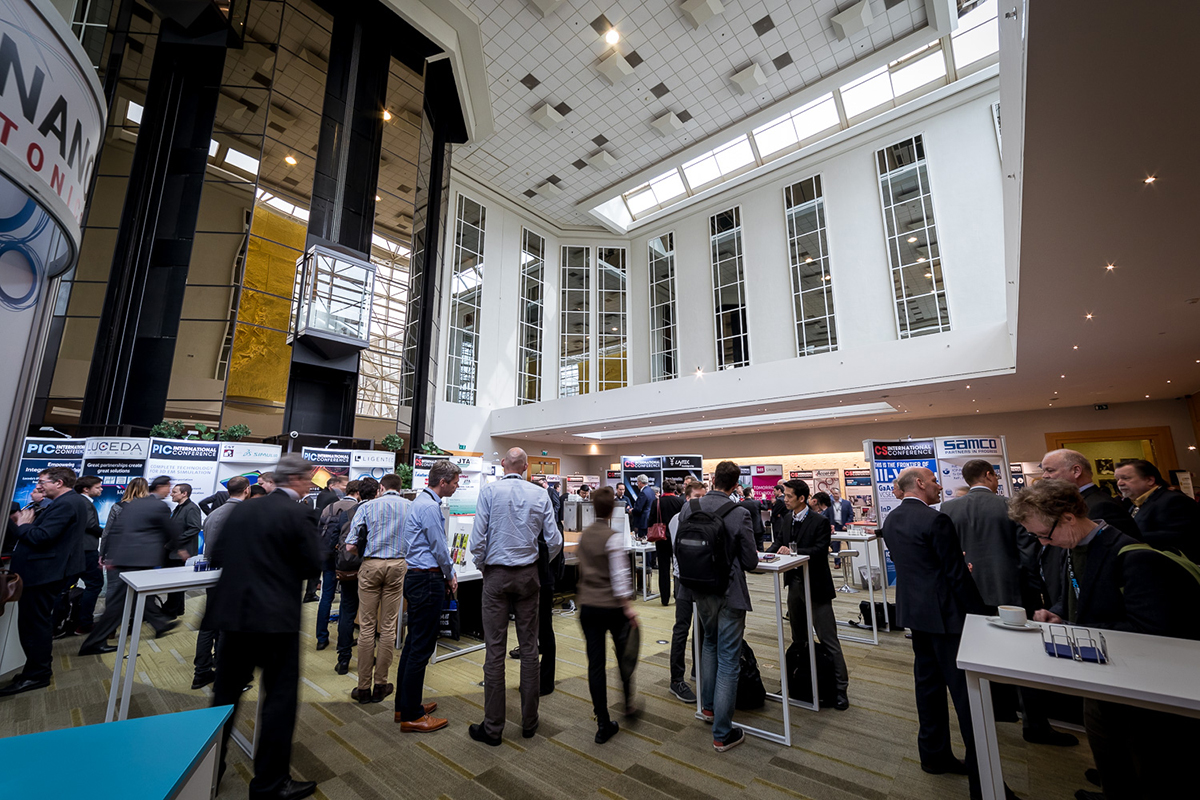
HES International recently concluded in Brussels, Belgium with a focus on advanced sensor technologies and applications of high-end sensors (HES) across many commercial and consumer market segments. Throughout the two-day program more than 600 attendees heard presentations from product and technology developers addressing opportunities in HES, photonic integrated circuits (PICs) and compound semiconductor (CS) technologies. Meeting rooms were packed as delegates and attendees circulated from one program to another, gaining insights into opportunities and challenges facing advanced IC innovators.
HES International and its focus on advanced sensing devices grew out of the successful Internet of Things (IoT) conference staged in 2017 alongside PIC and CS conferences. Throughout many IoT presentations, sensors quickly emerged as a common denominator in many IoT presentations, especially the most advanced devices still under development. This fact made it clear to conference organizers from Angel Business Communications that high-end sensors have rapidly become a linchpin technology that would continue to enable Smart City, Industry 4.0, flexible electronics, autonomous vehicle and many other other advanced applications that all share a common need to collect, analyze and communicate data with security and confidence.
Setting the tone on Day One of the conference was a keynote address by Olivier Sornique of Airbus, speaking about his role as Pressure Pad MEMS Projects Leader for flight test installations. Micro electromechanical system (MEMS) devices have emerged as one of the most versatile technologies for sensing a wide range of environmental and physical conditions as well as their well-established role as solid-state microphones.
Olivier told HES International delegates how Airbus utilized a range of commercially available MEMS devices in large volume to support a process the company describes as ‘measurement mapping’. Results to date have substantially surpassed previously available approaches, helping the company to ensure safety and reduce the time needed to conduct tests of new aircraft designs. Accuracy and repeatability of testing processes also increased substantially.
The successful integration of MEMS devices into a wide variety of high-end applications was a theme throughout the day. HES International attendees heard also from Bernhard Straub from Infineon Technologies who discussed ways that his company developed multiple generations of MEMS microphones for smartphone and related system applications. New core MEMS technology eliminated the issues Infineon had with legacy approaches for mobile sensing; the program now produces in excess of a billion devices annually with production expected to double or triple in the future.
Grenoble, France is home to CEA-Leti, one of the world’s largest research organization focused on advancing technology across many frontiers including high-end sensors. Leti’s efforts to develop and promote sensing technologies has led to a concentration of companies in the area, earning it the unofficial title of ‘Sensor Valley’ due to the fact that 10 of Europe’s largest advanced sensor developers are headquartered in and around Grenoble.
Sergio Nicoletti, coordinator of CEA-Leti’s MIRPHAB program, discussed optical sensor requirements and the important role that tunable lasers are expected to play in near-term product development as well as long range goals. He also detailed the role of MIRPHAB in helping new companies prototype devices while also conducting research into ways that sensors can decrease in size while consuming less power. Pierre-Damien Berger, also representing CEA-Leti, focused on the role of cyber physical systems (CPS) as enablers for high-end sensor development. Pierre-Damien spoke about the way that Leti has expertise in all aspects of developing microsystem and advanced sensors including MEMS, combining these for solutions tailored to the needs of various industry partners, helping manufacturers to identify and incorporate appropriate expertise into ongoing development programs. Their efforts include incubating new businesses, with six projects selected recently for continuing support and development activities.
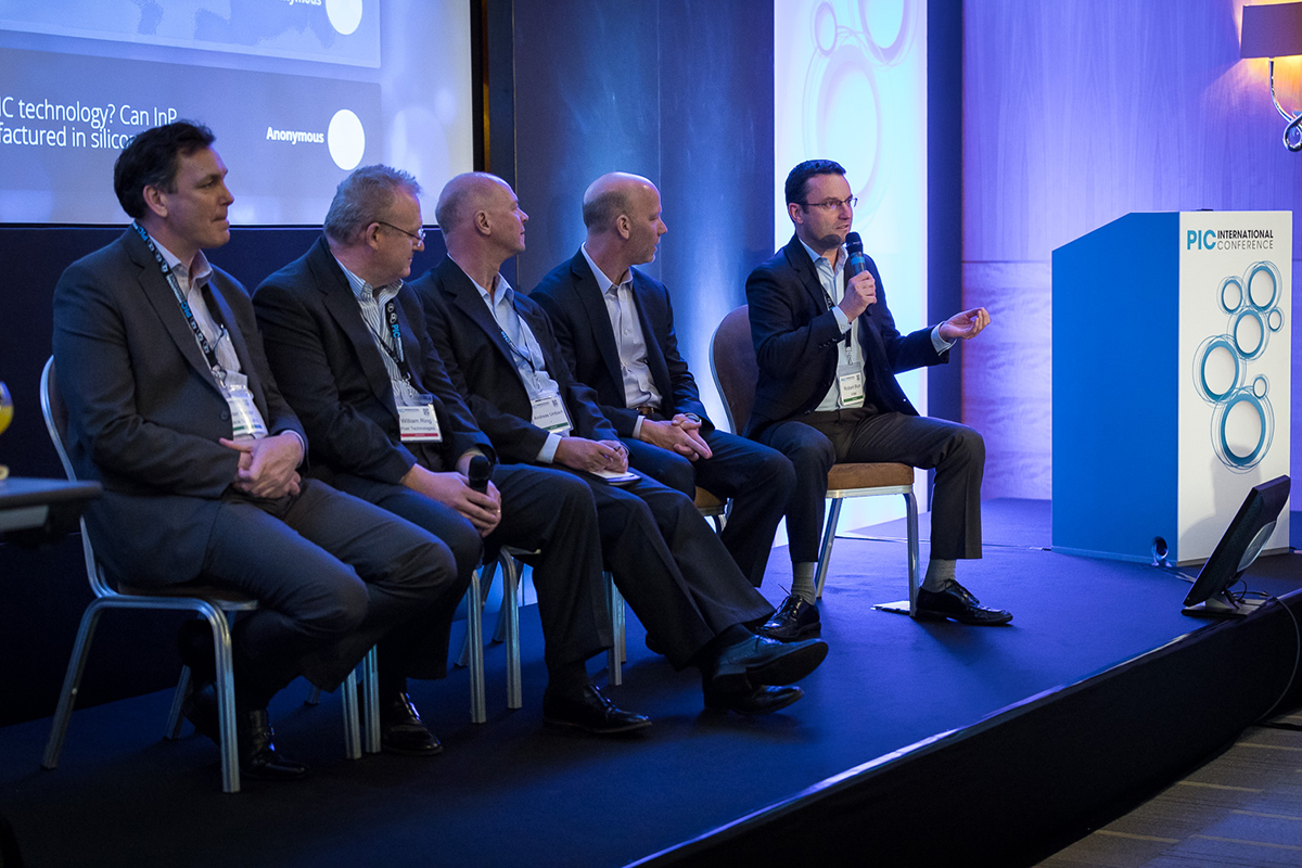
Throughout the conference it was clear that the dozens of companies represented see crossover opportunities and alignment between the capabilities of optoelectronic devices including fiber optic sensors and PICs with the advantages of silicon and compound semiconductor technologies. Work to bring together photon and electron based tech was typically seen as foundational to the ongoing development of high-end sensing devices.
Demonstrating the potential of fiber sensing was Pim Kat of Technobis. His company has utilized fiber optic sensing technologies to dramatically reduce the size (and cost) of sensory systems. Technobis fiber sensors have found their way into applications across automotive sectors including high-end racing vehicles and designs that are helping advanced marine telemetry and measurement applications. He remarked that the ability to replace traditional bulk modules with multiple discrete optical or micro-optical components with a single small-sized chip are making PICs an increasingly popular basis for next generation fiber sensing systems. Pim demonstrated how successful their approach has been by showing their corporate offices that have more than doubled in size since the company opened its doors.
While many companies are developing and marketing highly advanced sensors for applications across major commercial sectors, the need to package new devices is also becoming increasingly acute. New technologies that are radically smaller than legacy modules are typically manufactured utilizing existing semiconductor processes and fab equipment, and due to the size, power and connectivity requirements also need new approaches to packaging. Peter O’Brien of the Tyndall National Institute spoke about the institute’s endeavors to lead the charge into creating new packaging for emerging sensor technologies and increase market opportunities. Tyndall works with university and industry partners to essentially create new packaging approaches designed to enable prototyping as well as processes for transferring their new packaging expertise into volume production environments.
Also examining packaging and the underlying materials requirements of new technologies was Maurus Tschirky of Evatec. He examined the way that new materials pairings and layer stacks create new behaviors which need to be appreciated and understood across every stage of production. Optical interference coatings and work with piezoelectric layers were highlights of his presentation along with examples of ways in which materials science is playing an ever more significant roles as new sensors are created.
While optical and MEMS-based sensor technologies were the focus of many presentations, Mohamed Missous, professor of semiconductor materials and devices at the University of Manchester and CTO of Advanced Hall Sensors (AHS) reminded his audience that magnetic high performance devices offer substantial advantages compared to other underlying technologies. Quantum Well Hall Effect (QWHE) devices are the focus of his work, and Mohamed offered a fascinating look into the detailed resolution of QWHE devices that utilize AC and DC magnetic field scanning, enabling the detection of minute cracks in metals and in new applications that may replace security scanners with new generations of magnetic scanning tools that are more accurate while also reducing energy consumption and the amount of energy emitted when scans take place.
The enthusiasm and professionalism of presenters at HES International 2018 demonstrated the vital role and expanding opportunity for high-end sensors to drive the development of commercial and consumer products. Look for future articles that delve deeper into 2018 presentations as work towards an expanded 2019 program gets underway.